- 您现在的位置:买卖IC网 > Sheet目录317 > C8051T610DB24 (Silicon Laboratories Inc)DAUGHTER BOARD T610 24QFN SOCKET
�� �
�
�C8051T610/1/2/3/4/5/6/7�
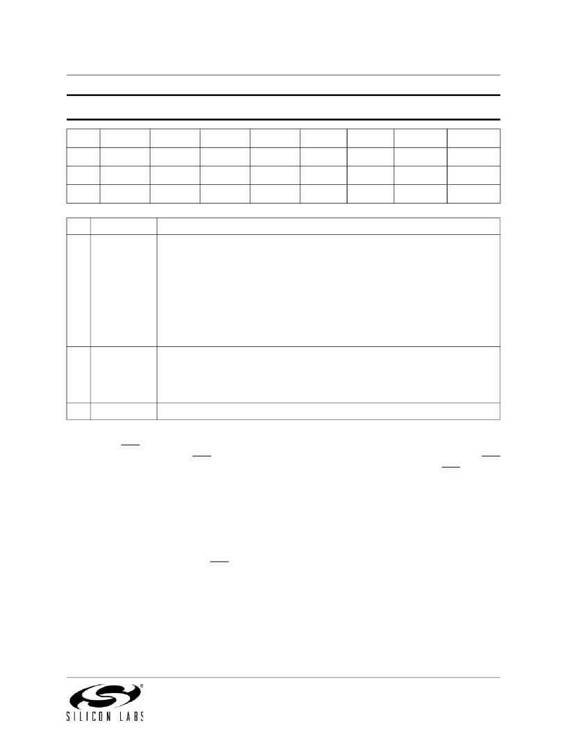
�SFR� Definition� 19.1.� VDM0CN:� V� DD� Monitor� Control�
�Bit�
�7�
�6�
�5�
�4�
�3�
�2�
�1�
�0�
�Name�
�VDMEN�
�VDDSTAT�
�Type�
�Reset�
�R/W�
�Varies�
�R�
�Varies�
�R�
�0�
�R�
�0�
�R�
�0�
�R�
�0�
�R�
�0�
�R�
�0�
�SFR� Address� =� 0xFF�
�Bit� Name�
�Function�
�7�
�6�
�5:0�
�VDMEN�
�VDDSTAT�
�Unused�
�V� DD� Monitor� Enable.�
�This� bit� turns� the� V� DD� monitor� circuit� on/off.� The� V� DD� Monitor� cannot� generate� sys-�
��inition� 19.2).� Selecting� the� V� DD� monitor� as� a� reset� source� before� it� has� stabilized�
�may� generate� a� system� reset.� In� systems� where� this� reset� would� be� undesirable,� a�
�delay� should� be� introduced� between� enabling� the� V� DD� Monitor� and� selecting� it� as� a�
�reset� source.� See� Table� 7.4� for� the� minimum� V� DD� Monitor� turn-on� time.�
�0:� V� DD� Monitor� Disabled.�
�1:� V� DD� Monitor� Enabled.�
�V� DD� Status.�
�This� bit� indicates� the� current� power� supply� status� (V� DD� Monitor� output).�
�0:� V� DD� is� at� or� below� the� V� DD� monitor� threshold.�
�1:� V� DD� is� above� the� V� DD� monitor� threshold.�
�Unused.� Read� =� 000000b;� Write� =� Don’t� care.�
�19.3.� External� Reset�
�The� external� RST� pin� provides� a� means� for� external� circuitry� to� force� the� device� into� a� reset� state.� Assert-�
�ing� an� active-low� signal� on� the� RST� pin� generates� a� reset;� an� external� pullup� and/or� decoupling� of� the� RST�
�pin� may� be� necessary� to� avoid� erroneous� noise-induced� resets.� See� Table� 7.4� for� complete� RST� pin� spec-�
�ifications.� The� PINRSF� flag� (RSTSRC.0)� is� set� on� exit� from� an� external� reset.�
�19.4.� Missing� Clock� Detector� Reset�
�The� Missing� Clock� Detector� (MCD)� is� a� one-shot� circuit� that� is� triggered� by� the� system� clock.� If� the� system�
�clock� remains� high� or� low� for� more� than� the� missing� clock� detector� timeout,� the� one-shot� will� generate� a�
�reset.� After� a� MCD� reset,� the� MCDRSF� flag� (RSTSRC.2)� will� read� 1,� signifying� the� MCD� as� the� reset�
�source;� otherwise,� this� bit� reads� 0.� Writing� a� 1� to� the� MCDRSF� bit� enables� the� Missing� Clock� Detector;� writ-�
�ing� a� 0� disables� it.� The� state� of� the� RST� pin� is� unaffected� by� this� reset.�
�Rev� 1.1�
�103�
�发布紧急采购,3分钟左右您将得到回复。
相关PDF资料
C8051T630DB20
BOARD SOCKET DAUGHTER 20-QFN
CAN-100
BOARD EVAL RS232 100QFP
CANADAPT28
KIT ADAPTER CANDEMOBOARD 28PLCC
CAT24AA01WI-GT3
IC EEPROM SERIAL 1KB I2C 8SOIC
CAT24AA02WI-G
IC EEPROM SERIAL 2KB I2C 8SOIC
CAT24C01ZI-G
IC EEPROM SERIAL 1KB I2C 8MSOP
CAT24C03WI-G
IC EEPROM SERIAL 2KB I2C 8SOIC
CAT24C04ZI-G
IC EEPROM SERIAL 4KB I2C 8MSOP
相关代理商/技术参数
C8051T610DB28
功能描述:子卡和OEM板 C8051T610 Family Socket Daughtr Board RoHS:否 制造商:BeagleBoard by CircuitCo 产品:BeagleBone LCD4 Boards 用于:BeagleBone - BB-Bone - Open Source Development Kit
C8051T610DB32
功能描述:子卡和OEM板 C8051T610 Family Socket Daughtr Board RoHS:否 制造商:BeagleBoard by CircuitCo 产品:BeagleBone LCD4 Boards 用于:BeagleBone - BB-Bone - Open Source Development Kit
C8051T610DK
功能描述:开发板和工具包 - 8051 C8051T610 Series Development Kit RoHS:否 制造商:Silicon Labs 产品:Development Kits 工具用于评估:C8051F960, Si7005 核心: 接口类型:USB 工作电源电压:
C8051T610-GQ
功能描述:8位微控制器 -MCU 16KB 10ADC 32Pin MCU RoHS:否 制造商:Silicon Labs 核心:8051 处理器系列:C8051F39x 数据总线宽度:8 bit 最大时钟频率:50 MHz 程序存储器大小:16 KB 数据 RAM 大小:1 KB 片上 ADC:Yes 工作电源电压:1.8 V to 3.6 V 工作温度范围:- 40 C to + 105 C 封装 / 箱体:QFN-20 安装风格:SMD/SMT
C8051T610-GQR
功能描述:8位微控制器 -MCU 16KB 10ADC 32Pin MCU RoHS:否 制造商:Silicon Labs 核心:8051 处理器系列:C8051F39x 数据总线宽度:8 bit 最大时钟频率:50 MHz 程序存储器大小:16 KB 数据 RAM 大小:1 KB 片上 ADC:Yes 工作电源电压:1.8 V to 3.6 V 工作温度范围:- 40 C to + 105 C 封装 / 箱体:QFN-20 安装风格:SMD/SMT
C8051T611-GM
功能描述:8位微控制器 -MCU 16KB 10ADC 28Pin MCU RoHS:否 制造商:Silicon Labs 核心:8051 处理器系列:C8051F39x 数据总线宽度:8 bit 最大时钟频率:50 MHz 程序存储器大小:16 KB 数据 RAM 大小:1 KB 片上 ADC:Yes 工作电源电压:1.8 V to 3.6 V 工作温度范围:- 40 C to + 105 C 封装 / 箱体:QFN-20 安装风格:SMD/SMT
C8051T611-GMR
功能描述:8位微控制器 -MCU 16KB 10ADC 28Pin MCU RoHS:否 制造商:Silicon Labs 核心:8051 处理器系列:C8051F39x 数据总线宽度:8 bit 最大时钟频率:50 MHz 程序存储器大小:16 KB 数据 RAM 大小:1 KB 片上 ADC:Yes 工作电源电压:1.8 V to 3.6 V 工作温度范围:- 40 C to + 105 C 封装 / 箱体:QFN-20 安装风格:SMD/SMT
C8051T612-GQ
功能描述:8位微控制器 -MCU 8KB 10ADC 32Pin MCU RoHS:否 制造商:Silicon Labs 核心:8051 处理器系列:C8051F39x 数据总线宽度:8 bit 最大时钟频率:50 MHz 程序存储器大小:16 KB 数据 RAM 大小:1 KB 片上 ADC:Yes 工作电源电压:1.8 V to 3.6 V 工作温度范围:- 40 C to + 105 C 封装 / 箱体:QFN-20 安装风格:SMD/SMT